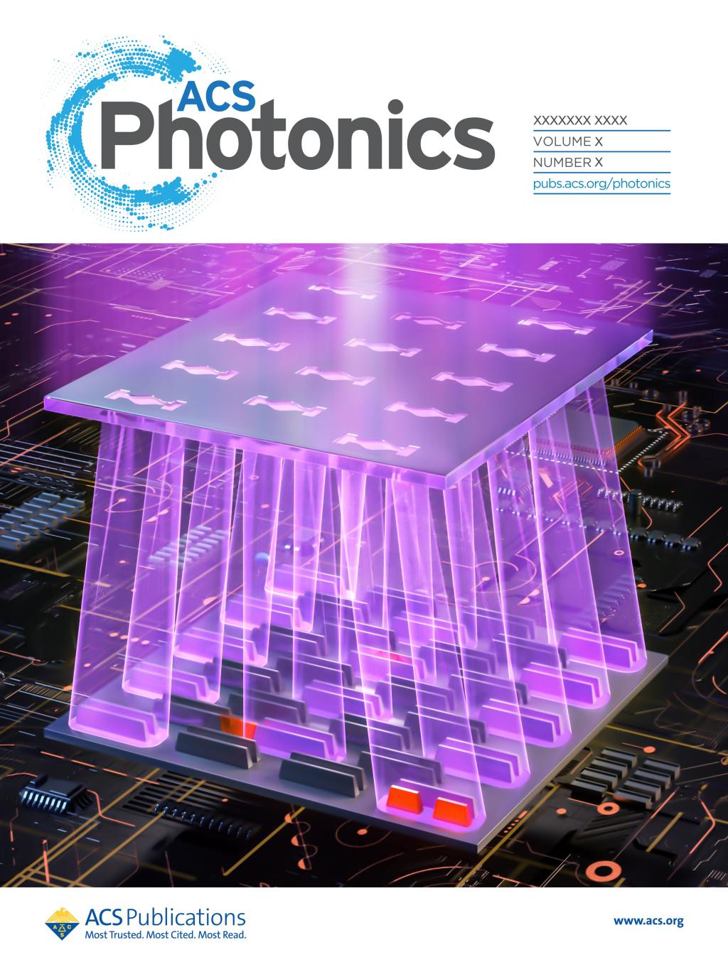
On September 6, the journal "ACS Photonics" affiliated with the American Chemical Society (ACS), published online a research paper authored by Prof. Shiyuan Liu and Prof. Jinlong Zhu from our institution. Their study employed custom structured light-field illumination on patterned wafers to precisely locate and categorize sub-wavelength defects in integrated circuits. The paper, titled "Optical Far-Field Detection of Sub-λ/14 Wide Defects by Conjugate Structured Light-Field Microscopy (c-SIM)," was chosen as the cover article. Jinsong Zhang, a doctoral student in our university's 2022 cohort, is the first author, with Prof. Shiyuan Liu and Prof. Jinlong Zhu as corresponding authors.


Detecting deep sub-wavelength defects in patterned wafers through label-free, non-destructive, real-time, and super-resolution detection using visible light illumination represents a significant challenge for defect inspection at advanced technology nodes. Conventional optical inspection methods are constrained by limited spatial resolution and the low signal-to-noise ratio of deep sub-wavelength defects within patterned wafers, making it unfeasible to detect these defects using visible light illumination. This is a prominent research issue in both the industry and academia.

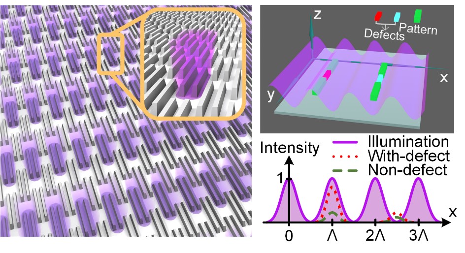
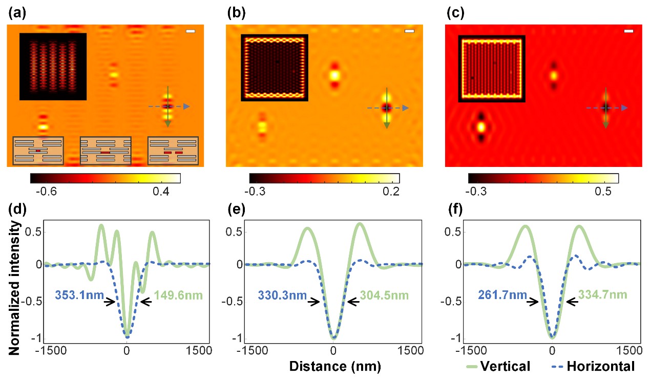
To overcome this challenge, the research team introduced a novel approach called Conjugate Structured Light-Field Microscopy. This method preserves the advantages of traditional bright-field microscopy, such as a large field of view, high efficiency, and non-destructiveness. Leveraging custom-optimized structured light-field illumination, this approach achieves precise localization and classification of sub-λ/14 wide defects within densely nanoscale features. In the paper, a set of densely packed two-dimensional periodic dual-line nanoscale patterns was taken as an example. By utilizing optical proximity correction methods to optimize the design of the illumination structured light-field, we simulated the detection of defects within the periodic patterns. Three different defects were successfully detected. Subsequently, by scanning the illumination position of the structured light-field, precise localization and classification of defects were achieved. The defects manifested as perturbation signals with enhanced resolution effects in the differential and gradient images, effectively doubling the resolution compared to traditional bright-field microscopy.

This research represents the first integration of optical proximity correction methods into the realm of defect detection. It enhances the defect localization precision of traditional optical microscopy and endows it with the ability to classify defects. The approach offers an efficient, non-destructive, easily integrable, and super-resolution method for defect inspection in patterned wafers.
Article link:https://pubs.acs.org/doi/10.1021/acsphotonics.3c00434